Microscopy standards
| Nanoscale AFM-CD Standard | Nanoscale Line Width / Grating Period Standard | AFM Tip Characterizer | ||
|---|---|---|---|---|
| Grating type: | 1-dimensional | x | x | x |
| 2-dimensional | x | |||
| circular | x | |||
| Line widths (nominal): | 50 nm – 80 nm | x | ||
| 80 nm – 300 nm | x | x | ||
| 300 nm – 800 nm | x | x | x | |
| 800 nm – 2 µm | x | |||
| Suitable for: | Optical microscopy | x | ||
| (deep ultraviolet microscopy) DUV, (confocal laser scanning microscopy) CLSM | x | |||
| Atomic force microscopy (AFM) | x | x | x |
AFM CD standard
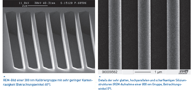
The nanoscale AFM-CD standard (CD, critical dimension) is based on etched silicon structures that allow the calibration of line widths and periods of AFM (atomic force microscopy) instruments.
This provides a set of very smooth and sharp-edged line gratings with vertical sidewalls, featuring minimum line widths of about 50 nm and depths of 250 nm, with high parallelism and deviations below 10 nm.
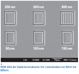
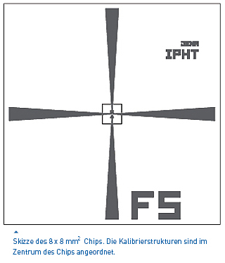
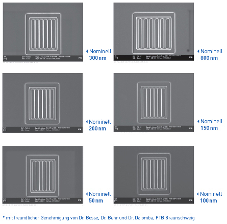
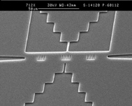
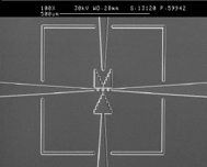
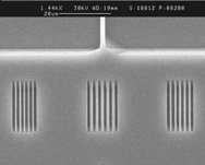
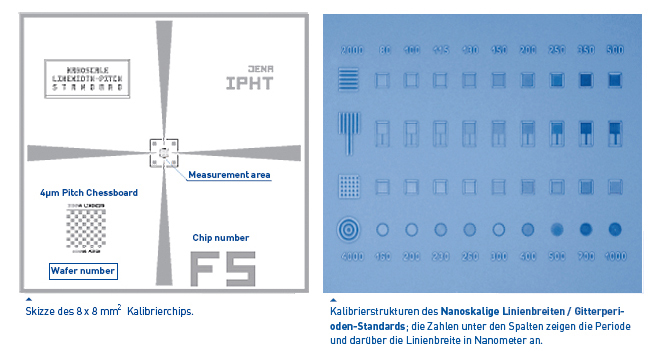
At the center of the 8×8 mm² calibration chips, two-level finder structures terminate, on which six groups of five-line gratings with various nominal widths (50, 100, 150, 200, 300, and 800 nm) are arranged.
The spacing between the lines is approximately 1 µm, and each group has a nominal length of 10 µm. In combination with the sharp-edged structures, edge radii of less than 15 nm are achieved, allowing for edge roughness below 5 nm (3σ).
Substrate Material: <110> Si Chip size: 8×8 mm² Surface accuracy: <1 nm Find structures Trenches in the Si substrate Depth: 250 nm Grid types 1-dimensional Grid size approx. 10×10 µm² Line widths (CD) nominal: 50 nm, 100 nm, 150 nm, 200 nm, 300 nm, 800 nm Line width deviation along the line (within a 1 µm long area): <3 nm 1σ Periods 1 µm + CD value Uncertainty of the main period: 3 nm 1σ Structure depth 250 nm Edge radius <15 nm Edge roughness <5 nm (p-p) Flank angle 89° AFM tip characterizer
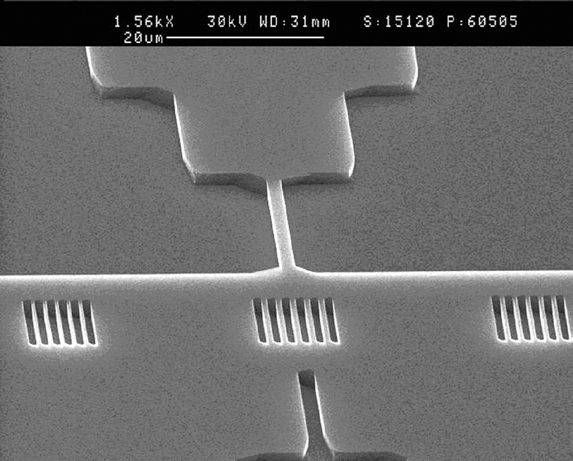
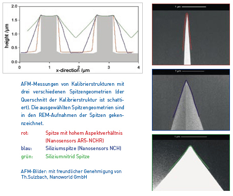
The layout for tip characterization includes a series of etched silicon line gratings with very smooth and sharp edges and vertical sidewalls.
Each calibration chip measures 8×8 mm². At the center of the chips, where the two-level finder structures end, three groups of five-line gratings with different nominal widths (300, 500, and 800 nm) are arranged. The spacing between the lines is approximately 1 µm, and each group has a nominal length of 20 µm.
The structures feature sharp edges with edge radii smaller than 2 nm, and the edge roughness is better than 5 nm (3σ).
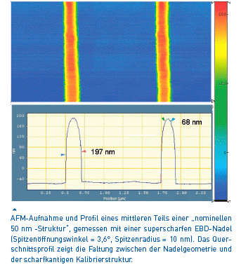
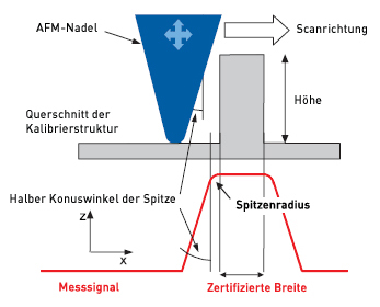
Substrate Material: <110> Si Chip size: 8×8 mm² Surface roughness: <1 nm Find structures Trenches in Si substrate·Depth: 1 µm Grid types 1-dimensional Grid size normally 10×10 µm² Line widths (CD) nominal: 300 nm, 500 nm, 800 nm Line width deviation along the lines (within a 10 µm long area): <5 nm 1σ Periods 1 µm + CD value Uncertainty of the main period: 3 nm 1σ Structure depth approx. 1 µm Edge radius <2 nm Edge roughness ± 4 nm (3σ) Flank angle 89° The method of in-situ characterization is based on AFM measurements of known line grating structures and the calculation of the tip geometry from the measurement results (see image).
Since the sidewalls of the calibration structures are steeper than half the cone angle of the probe tip, the measured structure sidewalls reflect the geometry of the AFM tip. If, in addition, the edge radius of the calibration structure can be neglected compared to the tip radius, the measured radii represent the actual radius of the AFM tip.Line width standard
The nanoscale line width / grating period standard provides various grating structures for line width calibration and resolution testing. It is particularly suitable for optical microscopy techniques such as DUV microscopy (deep ultraviolet microscopy) and CLSM (confocal laser scanning microscopy), as well as for AFM (atomic force microscopy). The etched structures in nanocrystalline silicon also allow for astigmatism testing.
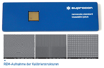
Due to the high optical contrast of the structures down to the UV wavelength range, the line width standard operates in UV transmission and UV reflection microscopy as well as in laser scanning microscopy with outstanding cost efficiency while maintaining precision. Available grating types include one-dimensional line gratings (for x and y) with a separate single structure for CD determination, as well as two-dimensional cross and circular gratings.
The period values for structure widths between 80 nm and 2 µm are 160, 200, 230, 260, 300, 400, 500, 700 nm, 1 µm, and 4 µm. Except for the larger 4 µm structures, each grating has an area of 10×10 µm².
Substrate Material: Quartz Chip size: 8×8 mm² Layer Nanocrystalline silicon Thickness: 25 nm Chip holder Dimensions: 76×26×2 mm Material: Aluminium alloy, anodised Find structures Au Thickness: 100 nm Grid types 1-dimensional (line grid for x+y) 2-dimensional (cross grid) circular (circle grid) a separate individual structure for CD determination on one side of the 1-dimensional grid Grid size normally 10×10 μm² Line widths (CD) nominal: 80 nm, 100 nm, 115 nm, 130 nm, 200 nm, 250 nm, 350 nm, 500 nm, 2 μm Line width deviation along the line (within a 6 μm long range): 8 nm 1σ Periods 160 nm, 200 nm, 230 nm, 260 nm, 300 nm, 400 nm, 500 nm, 700 nm, 1000 nm, 4 μm Uncertainty of the main period: 3 nm 1σ Roundness of the circular gratings ± 0.6 % deviation from the main period in the x and y directions (± 1 nm for 160 nm gratings) Maximum Resolution with DUV Microscope
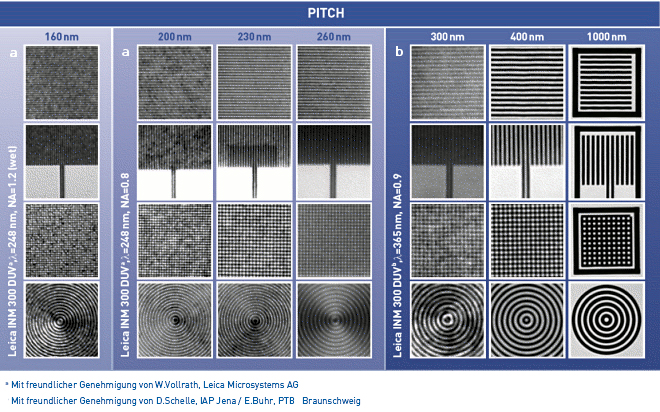
The DUV images show structures of the nanoscale line width / grating period standard captured using different objectives. The numbers above the columns represent the period in nanometers. Only high-resolution DUV microscopes (λ = 248 nm) with immersion objectives (NA = 1.2) provide such well-resolved images of the 160 nm grating.