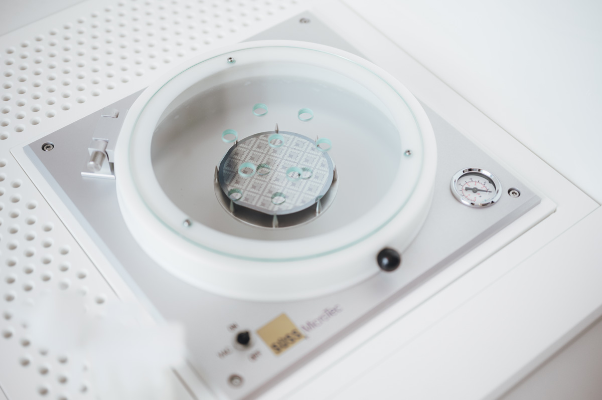
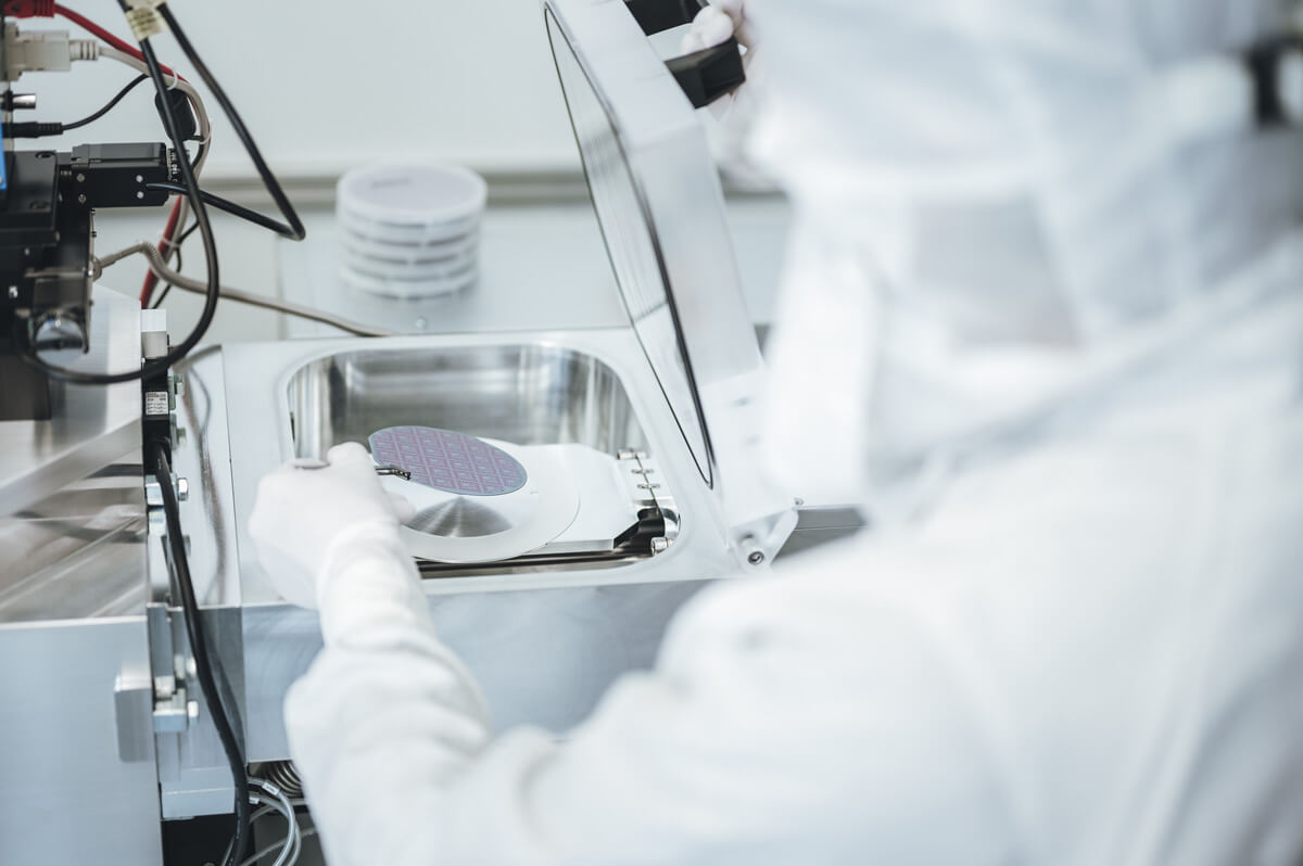
Coating
Thin films or multilayer systems made of metals, metal oxides, ceramic, and insulating materials such as silicon oxides can be deposited on various substrates. Supracon AG employs the following established methods:
- Resistive or electron beam evaporation
- Sputtering (DC, pulse-DC)
- Atomic Layer Deposition (ALD)
- Laser Ablation (PLD)
- Plasma Enhanced Chemical Vapour Deposition (PECVD)
SUBSTRATE SIZES AND MATERIALS ON REQUEST
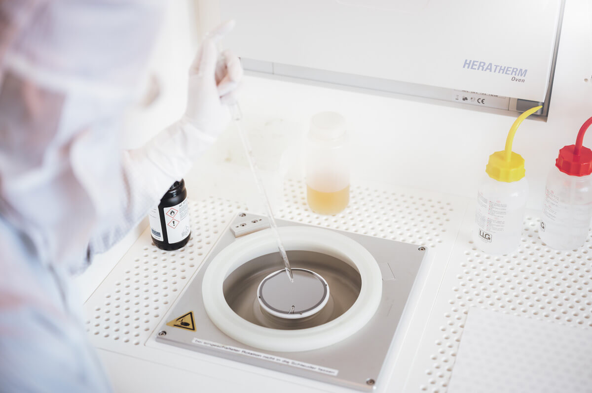
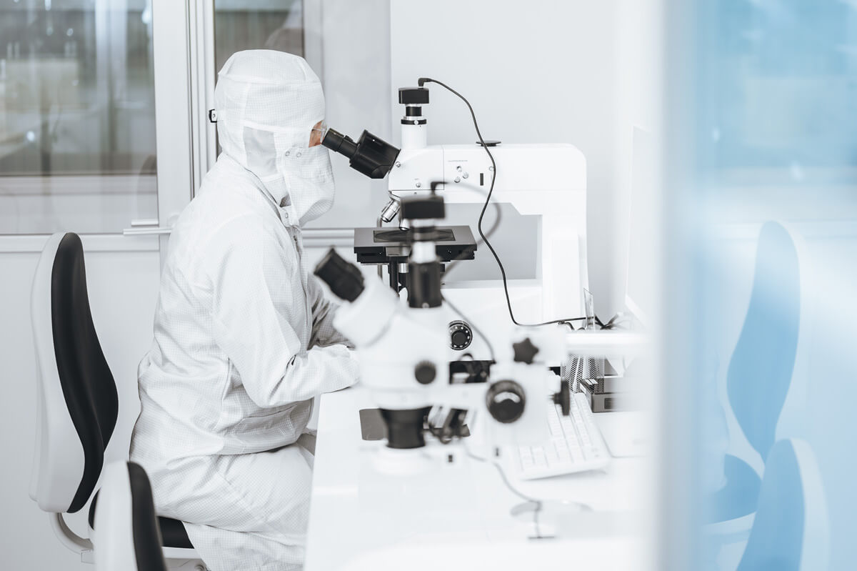
Lithography
Using different photoresists and corresponding baking processes, spin coating procedures can be performed.
Through projection exposure of photomasks, a wafer stepper transfers structures onto the prepared substrates. In a subsequent step, the resist structure is inspected under a light microscope using a developer solution.
Structure transfer
For this purpose, dry etching techniques such as RIE, IBE, and RIBE are available, as well as the lift-off technique.
In addition, wet etching processes can be used in silicon deep etching to create structures such as trenches and windows, exploiting different etching rates depending on the crystal orientation.
For all mentioned techniques, Supracon AG provides suitable masking solutions for the surfaces to be etched.
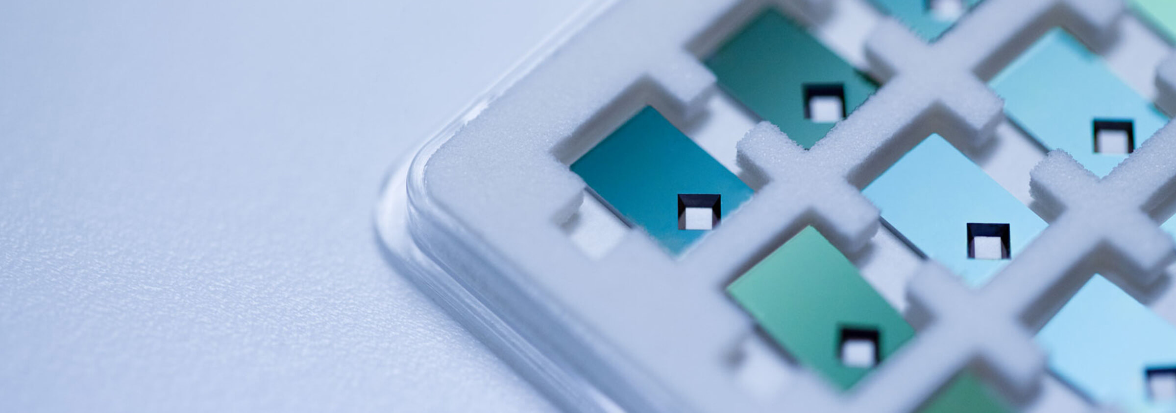
Assembly and interconnection technology
Mounting: Functional circuits or chips are mounted by gluing them onto chucks, printed circuit boards, or housing components.
Bonding: Using a manual wire bonder, the wiring of an integrated circuit or functional chip is connected to the electrical terminals of the housing or to other components.
Encapsulation: The chip is hermetically sealed in a housing and, if necessary, potted.